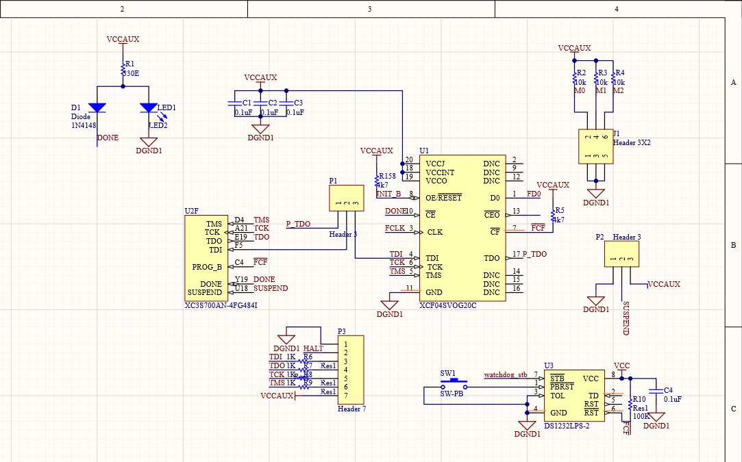
Schematic Design
The very starting point in electronic system design is Schematic. Schematic Design is an initial and important part of the rest of the design and development process. Mistakes in your schematic design can easily make their way all the way into prototypes or production without a second thought once the layout starts. Before the layout of schematics, design reviews are performed for their approval and often these tasks are time-consuming. Many times these schematic reviews still let many issues pass through which are not found until the prototype is tested, as all too many companies are too pressed for time to come up with a formal design review checklist relevant to their products.
The logical design partitioning, components annotation, alignment, polarities, connectivity between components, placement of components, electrical rule checks and net directives are important aspects that must be considered before transferring the design onto a PCB.
Schematic design is also helpful in finding out circuit behavior by simulation and then changing components type and model accordingly. We, at Tech Radix, provide you with complete Schematic Design Services which will help you in reducing the design errors and iterations.


PCB Design
Transferring your schematic circuit into a PCB is important for the successful functioning of the electrical circuit. But there are points that need to be considered before transferring the design such as :
1. Whether your schematic is able to transfer into the PCB layout.
2. Do all the footprints of all the components as per the requirements or availability.
3. Do all the nets connected and defined or labeled properly.
4. Have you defined the partitioning of your design like high voltage, power, communication, low speed, and high-speed sections.
5. Do all the track widths for the different nets properly chosen.
6. Is your grounding clear in your design.
7. The layer stack should be done prior to fabrication and in consultation with fabrication.
8. Are you following the standards.
All these points must be answered before laying out a circuit in the form of PCB. Fortunately, Tech Radix can answer these points as per your requirements and provide you circuit layout for your schematic design.
Circuit Design Documentation
The communication between teams of circuit designers and fabricators must be good to make your PCB as intended. The documentation, therefore, plays an important part that clearly communicates the fine details of the board other than files in standard electronic format such as Gerber or ODB++.
The design and schematic documentation which precisely details the design important points, considerations, corrections, and other information will not only be used for the manufacturer but also helpful in revisiting your designs and error to be avoided in the future.
The circuit documentation includes design details, fabrication details, dimensional details, hole and stack up details, and any other important point which will be either useful to the fabricator or may be required for later reference.


ECAD-MCAD Collaboration
ECAD and MCAD are different workings and unique areas. They bring different challenges when combined together. Although they are an important part of any system design, no collaboration between them can cause an increase in system cost by 50% or a delayed deadline.
Today’s system design requires complex PCB and complex enclosures from small to large products with irregular shapes enclosing various different and multiple designs or circuit boards. Multiple iterations of mechanical and electrical system collaboration are thus required before final fabrication with the help of ECAD-MCAD collaboration.
Therefore, visualizing your product’s electrical and mechanical collaboration before the final product will reduce design re-spin, cost, and time to market. Tech Radix will help you in designing your final product with ease.
Multi-board Design
Many times it happens that your system consists of multiple PCB boards with different connectors. Connecting these multiple boards connectors to connector alignment inside the mechanical enclosure is a challenging phase of the product development process. Without multiple considerations such as correct net assignment on each connector, connectors orientations on each board, connectors plugin fit, and height, and boards fitting into an enclosure, a mistake at this late stage of the product development cycle are costly, both for the cost of redesign and the delay to market. Planning multi-board system design & is a crucial and important part of complete system development. This will have the followings points to be considered:-
1- Determine board arrangement.
2- Choose connector.
3- Decide board functions.
4- Map signal across connectors.
5- 3D PCB Assembly.
We can help you in designing the systems which need multiple PCBs need to be arranged at one board with proper placement and positioning.

PCB design details input form
Contact us
It’s very easy to get in touch with us. Just use the contact form or pay us a visit for a coffee at the office. Dynamically innovate competitive technology after an expanded array of leadership.
Head Office
TECHRADIX PRIVATE LIMITED
104, Rituraj Business Center,
Bicholi Mardana, Indore, Madhya Pradesh 452016
- Phone: +91 89898 99596
- Email : info@tech-radix.com

